This tutorial shows you how to create the hardware equivalent of “Hello World”: a blinking LED. This is a simple exercise to get you started using the Intel® Quartus® Prime Software Lite edition software for FPGA development.
You’ll learn to compile Verilog code, make pin assignments, create timing constraints, and then program the FPGA to blink one of the four user LEDs on the board. You'll use a 50 MHz clock input (from the on-board oscillator) to drive a counter, and assign an LED to one of the counter output bits.
Level: Beginner
Materials
Hardware
Cyclone 10 LP kit
The Cyclone 10 LP Evaluation Kit is an easy-to-use platform to start development with Intel's low power Intel® Cyclone® 10 LP FPGA, and the Nios® II configurable 32-bit processor. You can buy the kit here.
Software
Intel® Quartus® Prime Software Suite Lite Edition
The FPGA design software used here is ideal for beginners as it’s free to download and no license file is required. You can download the software here.
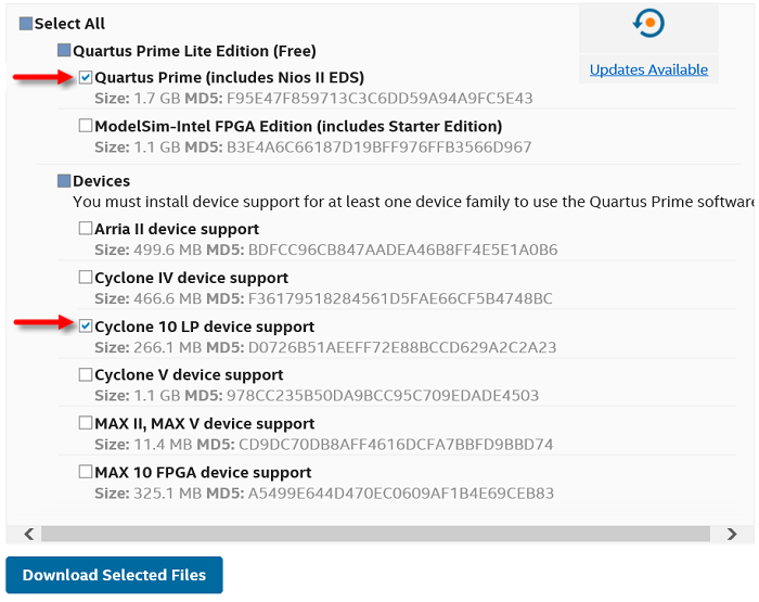
Note: The installation files are large (several gigabytes) and can take a long time to download and install. To minimize download time and disk space required, we recommend you download only those items necessary for this exercise. When prompted which files to download, uncheck “Select All” and select only Intel Quartus Prime and Intel Cyclone 10 LP device support only.
Once you’ve downloaded and installed the Intel® Quartus® software, you're ready to get started creating a project!
- Why is the Quartus download so big?
- The Quartus download contains several sophisticated tools to create a custom chip design, such as simulators, synthesis tools, place and route engines, timing analyzers, and device programmers, to name a few. Nearly all those functions are built into the Quartus Prime FPGA design software itself. The download also includes the embedded software design suite for the Nios II soft CPU, and one or more FPGA family databases - in our case the Cyclone 10 FPGA database.
Note: Screenshots are based on the latest release v17.0 User experience may vary when using earlier or later versions of Intel® Quartus® software.
Step 1: Create an Intel® Quartus® Software Project
Step 1.a: Open Intel® Quartus® Prime Software Suite Lite Edition.

Step 1.b: Open a New Project Wizard

Step 1.c: Select Next

Step 1.d: Directory, Name, Top-Level Entity
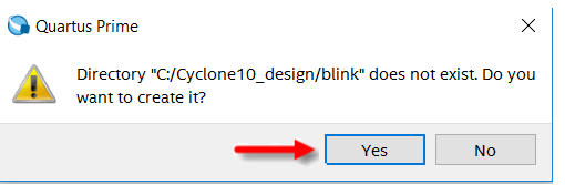
Choose a directory to put your project under. Here, we name our project “Blink” and place it under the intelFPGA_lite folder but you can place it wherever you want. Select Next.

When prompted to create the directory, choose Yes.
- Where should I put my future project files?
-
Here are a few guidelines you should adopt when choosing a directory for your project:
- Don’t put projects within the Quartus tool directory. New Quartus versions come out every six months, so placing them within a specific version directory will make them “orphans” once a new version is installed. Even worse, you might lose them if you delete the older tool version.
- Avoid paths with spaces in the name since some of the tools don’t like spaces in directory paths.
- Use directories where you have read/write access. This sounds intuitive, but sometimes IT departments limit administrator rights. Be sure the folder you create doesn’t require admin rights.
Step 1.e: Project Type
Select Empty Project, and then click Next.

Step 1.f: Add Files
You won’t be adding any files here. Click Next.

Step 1.g: Family, Device, and Board Settings (Note: You may need to expand window to view more device names)
Select the following:
Family: Cyclone 10 LP
Device name: 10CL025YU256I7G
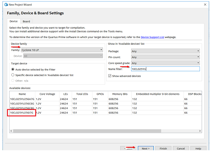
Click Next.
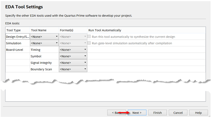
Step 1.h: EDA Tool Settings
We will be using the default EDA tools and settings so there are no changes to be made. Click Next.
Step 1.i: Summary
Click Finish

The following screen displays.

Step 2: Create an HDL File
Hardware Description Language (HDL)
We use Verilog as the HDL. If you are familiar with the C programming language but new to programming in an HDL, Verilog is like C in that you place a semicolon ‘;’ at the end of each statement.
Step 2.a: Navigate to the File tab (main window), and then select New.

Select Verilog HDL File, and then click OK.
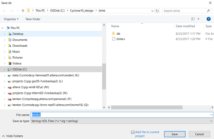
Step 2.b: Choose File > Save As. Choose “blink” for the file name. This is your top-level file name and it must match the name of the project name (blink). Click Save
Step 3: Create a Verilog Module
Step 3.a: Copy and paste this Verilog code into the blink.v window, and then save the file.
// create module
module blink (
    input wire clk, // 50MHz input clock
    output wire LED // LED ouput
);
// create a binary counter
reg [31:0] cnt; // 32-bit counter
initial begin
cnt <= 32'h00000000; // start at zero
end
always @(posedge clk) begin
cnt <= cnt + 1; // count up
end
//assign LED to 25th bit of the counter to blink the LED at a few Hz
assign LED = cnt[24];
endmodule

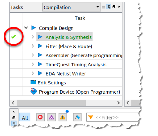
Step 3.b: Analysis & Synthesis
Right click on Analysis and Synthesis”, and then click Start to perform a syntax check and synthesis of the Verilog code.
- What happens during analysis and synthesis?
-
The Analysis & Synthesis process:
- Checks design files for syntax and semantic errors
- Performs netlist extraction to build a database which integrates all the design files
- Synthesizes the hardware description language (HDL) code into hardware blocks appropriate for the target FPGA family
If the process completes successfully, a green check mark displays next to Analysis & Synthesis. If you get an error, check your syntax and make sure it matches exactly the code block provided above. Be sure you used the “View Source” button when you copied the text in step 3.a above.
Step 4: Choose Pin Assignments
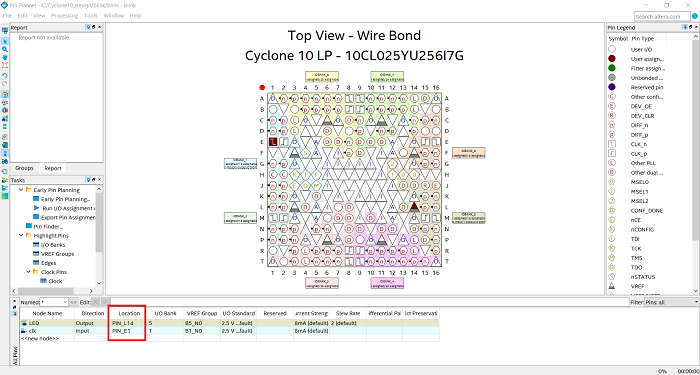
Step 4.a: In the top navigation bar, select Assignments > Pin Planner.

Step 4.b: One at a time, click to highlight the Location column for each pin, then type the pin location for the LED and clk signals as shown below. The rest of the columns will auto populate with data (some with default values that we’ll modify in the next step).
| Node Name | Location |
|---|---|
| LED | PIN_L14 |
| clk | PIN_E1 |
You also need to change the I/O standard, Current Strength and Slew Rate columns from their default settings to the values shown below:
| Node Name | Location | I/O Standard | Current Strength | Slew Rate |
|---|---|---|---|---|
| LED | PIN_L14 | 3.3-V LVTTL | 8ma | 2 |
| clk | PIN_E1 | 2.5V | 8ma |
Step 4.c: To change the I/O standard, double click each cell and a pull-down menu will appear. Click the down arrow icon and scroll to the desired value. Change the I/O standard from the default 2.5V to 3.3-V LVTTL.
Step 4.d: Leave the Current Strength for the LED output to 8ma(default) for both input (clk) and output (LED).
Step 4.e: Leave the Slew Rate for the LED output to 2(default). You don’t need to set a Slew Rate for the clk. Leave that blank

Step 4.f: Close the Pin Planner.
Step 5: Create an SDC File
Before you compile the Verilog code, you need to provide timing constraints for the design. You'll create an SDC (Synopsis Design Constraints) file that contains commands to let the Intel® Quartus® software know how to close timing on the design. Without it, you will get warning messages in the compile flow because the Intel® Quartus® software has no idea how to close timing on the design.
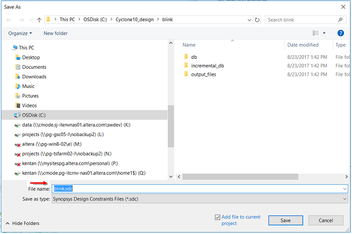
To create a blink.sdc and add it to the blink file directory, do the following.
Step 5.a: Navigate to the File tab (main window), and then select New.

Select Synopsys Design Constraints File, and then click OK.
Step 5.b: Choose File > Save As. Choose “blink.sdc” for the file name. Click Save
Copy and paste the following content into the blink.sdc window, and then save the file.
# inform Quartus that the clk port brings a 50MHz clock into our design so
# that timing closure on our design can be analyzed
create_clock -name clk -period "50MHz" [get_ports clk]
# inform Quartus that the LED output port has no critical timing requirements
# it’s a single output port driving an LED, there are no timing relationships
# that are critical for this
set_false_path -from * -to [get_ports LED]- What is an SDC file, and why do I need one?
-
SDC stands for Synopsys Design Constraints and is an industry standard format which defines the timing constraints for a hardware (silicon) design such as the target frequency of the device, and the timing to external peripherals. The SDC file provides a way for Quartus to verify that the system generated meets its timing requirements.
During synthesis of your FPGA, a design tool called TimeQuest is called by Quartus which reads the timing constraints files, calculates the timing of the internal FPGA signals, and compare these timings to the timing requirements specified by the SDC files. A report is created which verifies timing is met and / or identifies signals which fail to meet timing and require optimization.
Step 6: Compile the Verilog Code
Step 6.a:
Right click on Compile Design, and then click Start. The tools will then synthesize, place and route, assemble and perform timing analysis on the design Because there are only have a handful of code lines, the compilation should only take a couple of minutes to complete.
- What happens during the fitter (place & route)
-
The Fitter places and routes the logic of your synthesized design into target device resources. Think of it like a router that lays out a printed circuit board, connecting the various devices together using copper traces. In this case, however, the devices are logic resources (e.g. lookup tables, registers, memories, multipliers, etc.) and the traces are routing “wires” inside the FPGA device.
- What happens during the assembler?
-
The Assembler generates a programming image from a successful fit which can then be downloaded to the FPGA device.
- What is timing analysis?
-
Timing analysis is the process of evaluating the timing of logic in the device after it has been synthesized, placed and routed to ensure the all timing requirements are met. The goal is to achieve “timing closure” where all the timing constraints are met.

After compilation is complete you will see a summary report like the one below.

After you compile the Verilog code, you can program the FPGA.
Step 7: Program the FPGA
The final step is to program the FPGA.
Step 7.a: Connect the board to your computer via the USB blaster port. Use the USB cable (mini-b connector) that came with the “unknown” kit. Insert the mini-b connector into the USB Blaster port (J17) on the “unknown” board and the Type-A end into a standard USB port on your host computer.
Step 7.b: Connect the board to power and verify there is a blue LED lit near the J13 USB Blaster II port.
Step 7.c: Right click to open Program Device.

Step 7.d: Hardware Setup
Select Hardware Setup
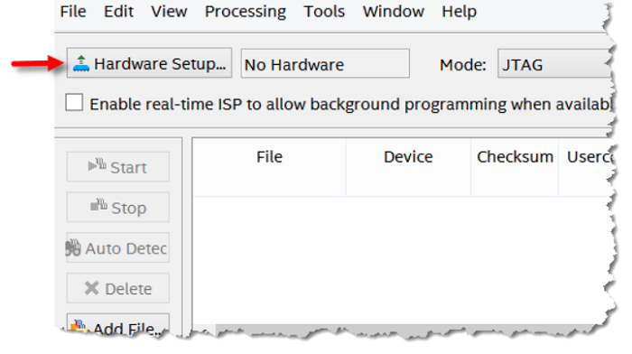
Under the drop down for Currently selected hardware, choose Cyclone 10 LP Evaluation Kit [USB-1], then click Close.

Step 7.e: Click Auto Detect to identify the JTAG chain on the board.

Select the device 10CL025Y. This is the FPGA device.

Step 7.f: Add the .sof file.
Right click on the File column for the 10CL025Y device and select Change File.

Step 7.g: Navigate to the output_files folder, select blink.sof, and then click Open.

Here, blink.sof is your programming file. SRAM Object Files (.sof files) are binary files containing data for configuring SRAM-based devices—our FPGA is based on SRAM—using the Intel® Quartus® software Program Device (also called Programmer). The programmer looks into the SOF file and gets the programming bit stream for the device.
Step 7.h: Check the Program/Configure column, and then click Start.

Step 8: Observe the blinking LED
If your progress bar is 100% (Successful), watch LED0 blinking.


Experiment on Your Own
Change the Blink Rate
Now that you’ve got one successful blinking LED under your belt, you can modify the blink rate of the LED by using a different “bit” of the counter. 1 Hertz is 1/second (cycles per second) and blinking at 1 Hz means the LED blinks once per second. For 2 Hz, the LED blinks twice per second. And 0.25 Hz would blink the LED once every 4 seconds (slow blink). For a slower blink, use a higher bit of the counter and for faster, use a smaller bit (e.g., cnt[22]). Test out different counter bits and see what you get.
Clock and Counter Math
cnt[n] where n = the counter bit
2^n; we've chosen n = 24 in our Verilog code sample
2^24 = 16,777,216
Our clock is 50 MHZ or 50,000,000
Clock / 2^n = blinks per second
50,000,000 / 16,777,216 = 2.9802
That’s about 3 blinks per second.
To make this change, you will need to:
- Modify the Verilog file (blink.v) and select a different counter bit in the assignment statement.
- Recompile the design
- Reprogram the FPGA
Add More LEDs
Try connecting one or more of the remaining 3 LEDs to other counter bits, with each blinking at a different rate. For example, you could add a new LED connected to counter bit 23 which would blink twice as fast as bit 24. Or you could add all the remaining 3 LEDs and connect each to a unique counter bit.
To make this change, you will need to:
- Modify the Verilog code (step 3a):
- Add the new LEDs to the module definition
- List the new LEDs as being outputs
- Assign each of the new LEDs to a unique counter bit (cnt[n])
- Run Analysis and Synthesis (step 3b)
- Assign the LEDs outputs to pins using the Pin Planner (steps 4b - 4e).
Be sure to set the proper I/O standard, drive strength, and slew rate. The I/O pin connected to the LEDs are as follows:
LED0: PIN_L14
LED1: PIN_K15
LED2: PIN_J14
LED3: PIN_J13
- Recompile the design (step 6a)
- Reprogram the device (step 7h)